Gallium Nitride (GaN) has transformed high-power and high-frequency electronics. From RF amplifiers and radar systems to satellite communications, 5G infrastructure and advanced power electronics, GaN devices can operate at power densities and frequencies that are difficult to achieve with conventional silicon technologies.
But higher power density creates a fundamental challenge:
Heat.
As GaN devices become more powerful and compact, removing heat from the active region becomes increasingly important. Excessive junction temperature can reduce performance, limit achievable power density and affect long-term device reliability.
One promising approach is GaN-on-Diamond — bringing one of the world’s highest-performing thermal materials extremely close to the heat-generating GaN device.
Why Does GaN Have a Thermal Challenge?
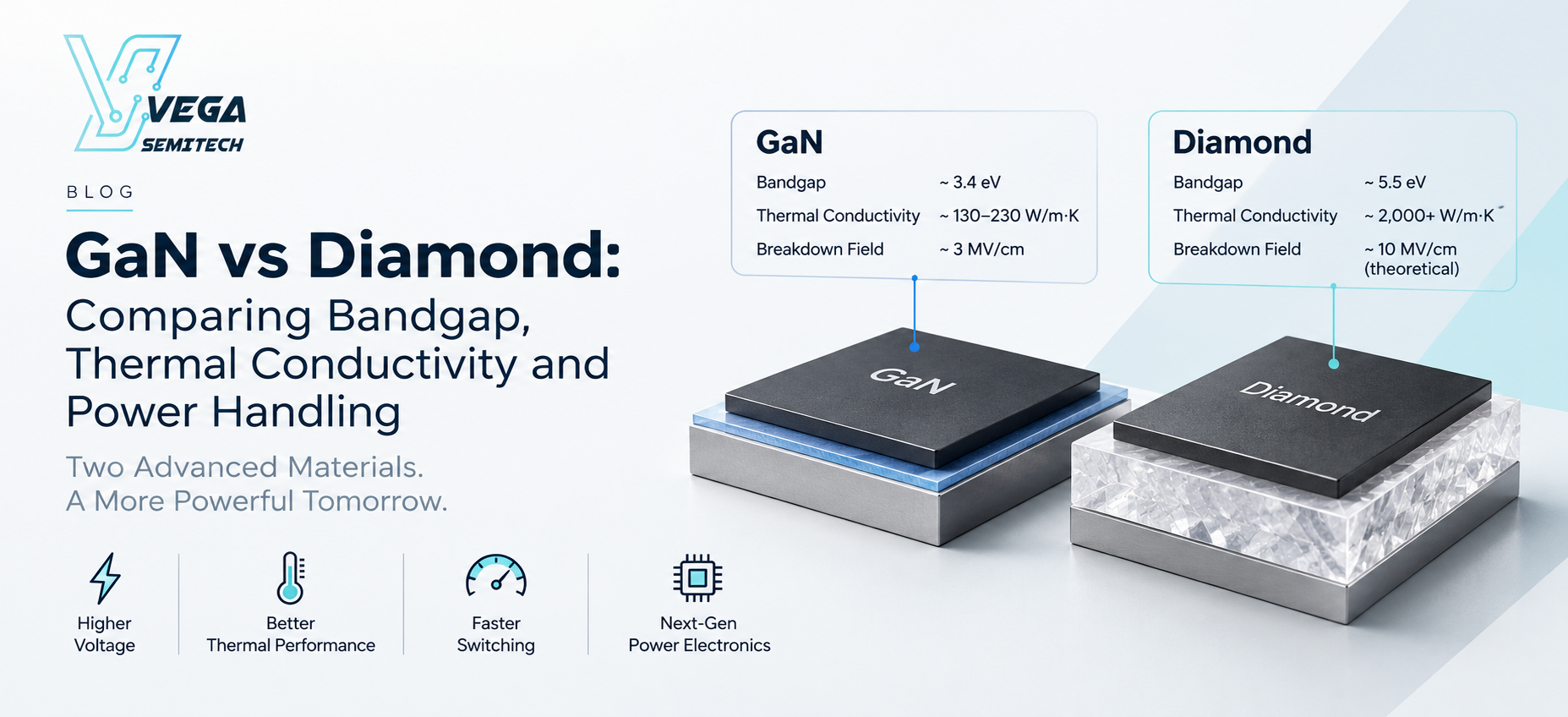
GaN offers several important advantages for high-performance electronics, including a wide bandgap, high breakdown field and high electron mobility.
These properties make GaN particularly attractive for high-power and high-frequency devices.
However, high performance also means that significant heat can be generated within a very small device area.
In a GaN HEMT (High Electron Mobility Transistor), localized hotspots can develop near the transistor channel and gate region. The challenge is therefore not simply cooling the overall package.
The heat needs to be moved away from the active region of the device as efficiently as possible.
A conventional thermal path may look like:
GaN Active Region → GaN Layer → Substrate → Package → Heat Sink → Cooling System
Every material and interface along this path contributes thermal resistance.
The longer and more thermally resistive this path becomes, the harder it is to control the device temperature.
Why Diamond?
Diamond is widely recognized as an exceptional thermal-management material.
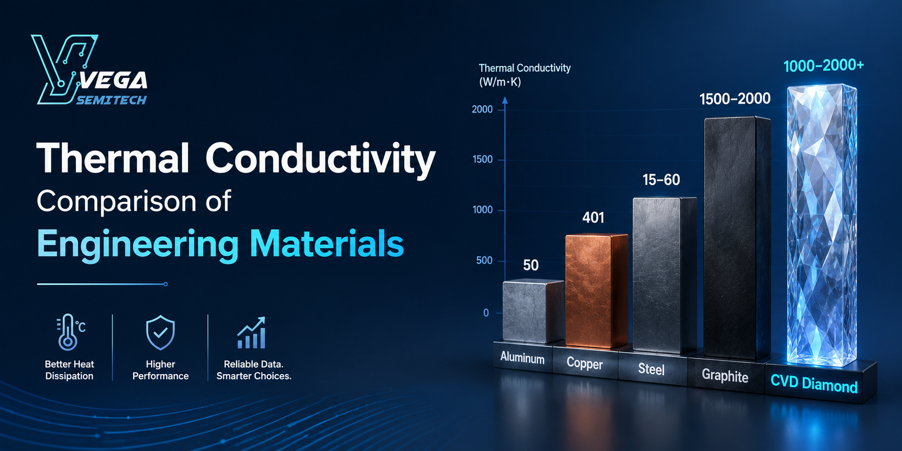
High-quality engineered CVD diamond can achieve extremely high thermal conductivity, significantly exceeding many conventional semiconductor substrate and packaging materials.
This makes diamond particularly interesting for devices where a large amount of heat must be removed from a very small area.
Instead of simply placing a better heat sink farther away from the semiconductor, GaN-on-Diamond aims to bring the thermal solution much closer to where the heat is generated.
What Is GaN-on-Diamond?
GaN-on-Diamond is an advanced semiconductor architecture in which GaN device layers are integrated with a diamond substrate or diamond thermal layer.
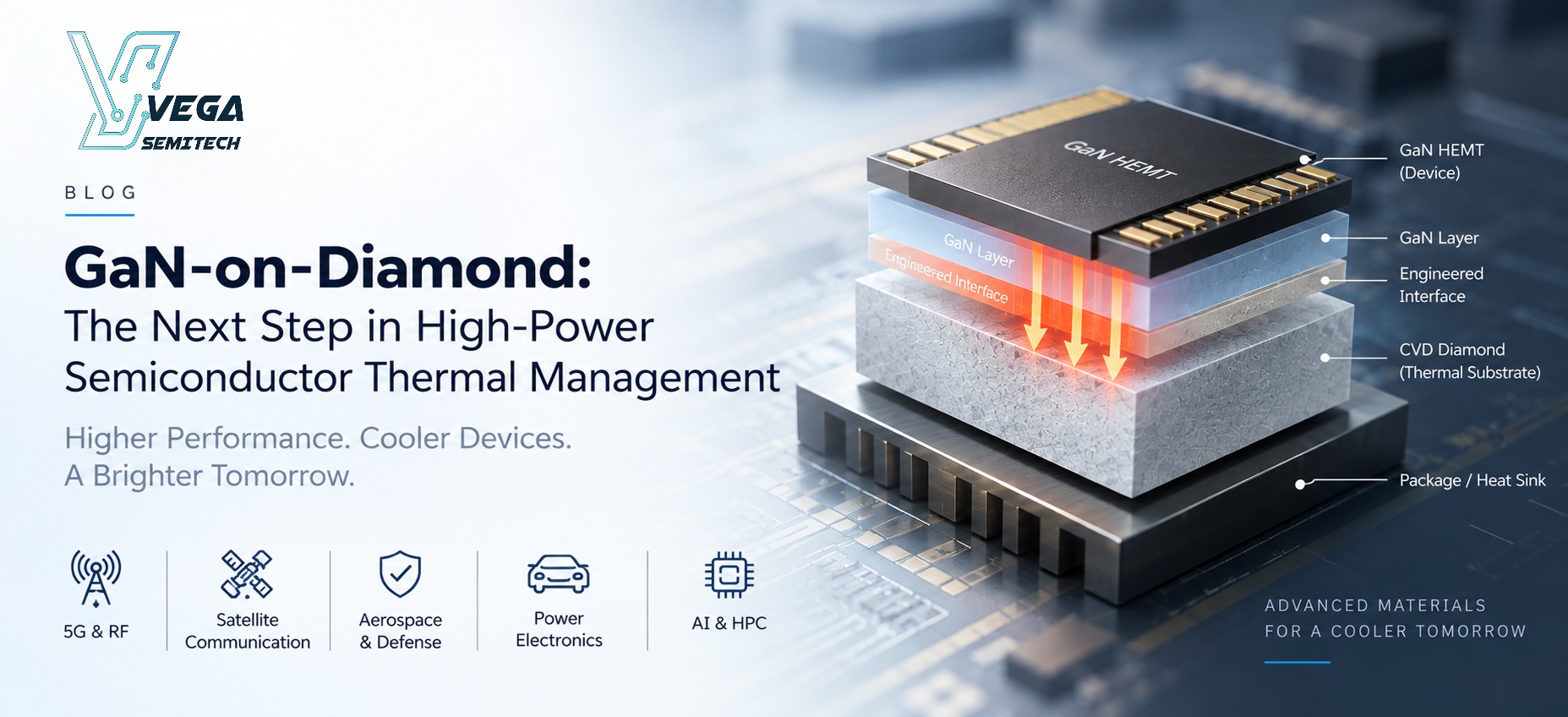
A simplified structure can be represented as:
GaN Device / HEMT
↓
GaN Active Layer
↓
Engineered Interface
↓
CVD Diamond
↓
Package / Thermal Management System
Heat generated inside the GaN device can travel through a relatively short thermal pathway into the highly thermally conductive diamond.
The diamond then rapidly spreads the concentrated heat over a larger area.
This can make it easier for the package, heat sink or cooling system to remove the heat.
Why Bring Diamond Closer to the GaN Device?
Consider a very small hotspot generating a large amount of thermal energy.
Even if a powerful cooling system is installed at the package level, heat must still travel from the transistor through multiple material layers before reaching that cooling system.
This creates a thermal bottleneck.
GaN-on-Diamond attempts to address the problem at its source.
Traditional approach:
GaN → Substrate → Package → Thermal Interface → Heat Sink
GaN-on-Diamond approach:
GaN → Engineered Interface → Diamond → Package → Cooling
The objective is to reduce thermal resistance close to the active device and spread heat before it becomes concentrated within the package.
Potential Benefits of GaN-on-Diamond
Effective integration of GaN and diamond could offer several important benefits.
Lower Device Temperature
Improved heat extraction can help reduce the temperature of the active device region.
Lower junction temperatures can be valuable for both performance and reliability.
Higher Power Density
Thermal limitations can restrict how much power a semiconductor device can practically handle.
Better thermal management may allow engineers to explore higher device power densities without allowing temperature to become the dominant limitation.
Improved Reliability
Repeated operation at elevated temperatures can accelerate degradation mechanisms within semiconductor devices and packaging.
Controlling operating temperature can therefore contribute to improved long-term reliability.
Smaller and Lighter Systems
If heat can be removed more effectively at the device level, future systems may be able to reduce their dependence on large thermal-management structures.
This is particularly attractive for aerospace, satellite and defense applications where size and weight are critical.
Better RF Performance
GaN HEMTs are widely used for high-frequency RF applications.
Self-heating can influence electrical characteristics and device performance. Improved thermal management can help devices maintain more consistent performance under demanding operating conditions.
Applications for GaN-on-Diamond
The combination of GaN’s electronic performance and diamond’s thermal performance makes the technology particularly interesting for demanding applications.
RF and 5G/6G Infrastructure
GaN is already widely used in high-power RF systems.
Future wireless networks will continue demanding greater bandwidth, higher frequencies and increased power efficiency.
Improved thermal management could help GaN RF devices operate at higher power densities while maintaining temperature control.
Radar and Defense Electronics
High-power radar systems require RF devices capable of operating under extreme conditions.
GaN-on-Diamond could potentially support higher-performance radar electronics while helping reduce thermal constraints.
Satellite Communications
Space systems place a premium on performance, reliability, size and weight.
Efficient device-level thermal management is therefore particularly valuable for satellite RF and communication systems.
Aerospace
Aircraft and advanced aerospace platforms increasingly depend on compact, high-performance electronic systems.
Diamond-based thermal management could help enable smaller and more power-dense electronic architectures.
High-Power Electronics
Beyond RF, GaN continues to expand into power conversion and other high-power electronic applications.
As device power density increases, advanced thermal materials may become increasingly important.
The Interface Is the Critical Engineering Challenge
Simply combining GaN and diamond does not automatically produce an ideal thermal device.
One of the most important challenges is the GaN–Diamond interface.
Heat must cross this interface before it can benefit from diamond’s high thermal conductivity.
If the interface has high thermal boundary resistance, it can become a bottleneck itself.
Engineers therefore need to carefully control factors including:
- Diamond material quality
- Interface thickness
- Surface preparation
- Bonding technology
- Intermediate layers
- Thermal boundary resistance
- Mechanical stress
- Coefficient of thermal expansion
- Wafer uniformity
- Device-processing compatibility
This means GaN-on-Diamond is not simply a materials problem.
It is a combination of materials science, semiconductor processing, interface engineering and thermal design.
Single-Crystal or Polycrystalline Diamond?
Different GaN-on-Diamond architectures may require different forms of engineered diamond.
Single-Crystal Diamond (SCD) offers excellent material properties and very high thermal performance, making it attractive for specialized high-performance applications.
Polycrystalline Diamond (PCD) can offer advantages for larger-area thermal solutions and potentially more scalable manufacturing.
Selecting the appropriate diamond material depends on factors such as device architecture, required thermal performance, wafer size, manufacturing process and target cost.
As the technology develops, both SCD and PCD can have important roles within the semiconductor ecosystem.
GaN-on-Diamond vs Conventional GaN Substrates
GaN devices are commonly developed using substrates and material systems such as silicon, silicon carbide and sapphire, depending on the application.
These platforms have established manufacturing ecosystems and important advantages.
GaN-on-Diamond should therefore not be viewed simply as a replacement for every existing GaN technology.
Instead, it is particularly interesting for applications where thermal performance becomes one of the primary constraints on device performance.
The question changes from:
“Which substrate is cheapest or easiest to manufacture?”
to:
“How much more performance could the device deliver if heat were no longer its primary limitation?”
That is where diamond becomes especially interesting.
From Heat Spreaders to Semiconductor Integration
Diamond thermal management can exist at several levels within an electronic system:
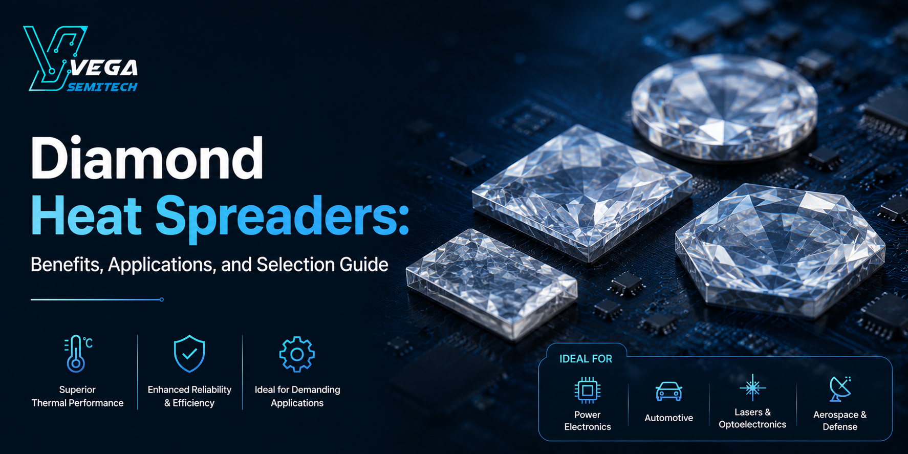
Level 1 — Diamond Heat Spreader
Diamond is incorporated into the package to spread heat.
Level 2 — Diamond Substrate
Diamond is positioned directly beneath semiconductor device structures.
Level 3 — GaN-on-Diamond
GaN and diamond are closely integrated to minimize the thermal distance from the active device.
The industry is progressively exploring ways to bring high-performance thermal materials closer to the heat source.
GaN-on-Diamond represents one of the most advanced forms of this strategy.
Vega Semitech and the Future of GaN-on-Diamond
At Vega Semitech, our focus is on developing advanced diamond materials and semiconductor technologies for next-generation electronic systems.
Our work across single-crystal diamond, polycrystalline diamond, diamond heat spreaders, advanced thermal materials and GaN-on-Diamond is aimed at addressing one of the semiconductor industry’s most important challenges: thermal management.
As semiconductor devices continue moving toward higher frequencies, higher power densities and smaller form factors, simply improving external cooling may not be enough.
The thermal solution must move closer to the semiconductor itself.
GaN provides exceptional electronic performance.
Diamond provides exceptional thermal performance.
Bringing the two together could help unlock the next generation of high-power semiconductor devices.
GaN-on-Diamond: Electronics Meet Thermal Engineering
The future of semiconductor performance will not be determined only by how quickly electrons can move or how efficiently a transistor can switch.
It will also depend on how quickly the heat can move away.
GaN-on-Diamond represents a powerful convergence of semiconductor engineering and advanced thermal materials — and an important pathway toward cooler, smaller and more powerful electronic systems.