As semiconductor devices become smaller, faster and more powerful, one challenge is becoming increasingly difficult to manage: heat.
Modern AI processors, RF power amplifiers, GaN devices, SiC power electronics, laser systems and high-performance computing hardware operate at increasingly high power densities. This means a significant amount of heat can be generated within a very small area of the device.
Traditional cooling systems can remove heat from the package, but before that happens, heat must first travel efficiently away from the semiconductor die.
This is where diamond heat spreaders can play an important role.
What Is a Diamond Heat Spreader?
A diamond heat spreader is a thin layer, plate or substrate of engineered diamond material positioned close to a heat-generating semiconductor device.
Its primary purpose is simple:
Move heat away from a concentrated hotspot and spread it across a larger area as quickly as possible.
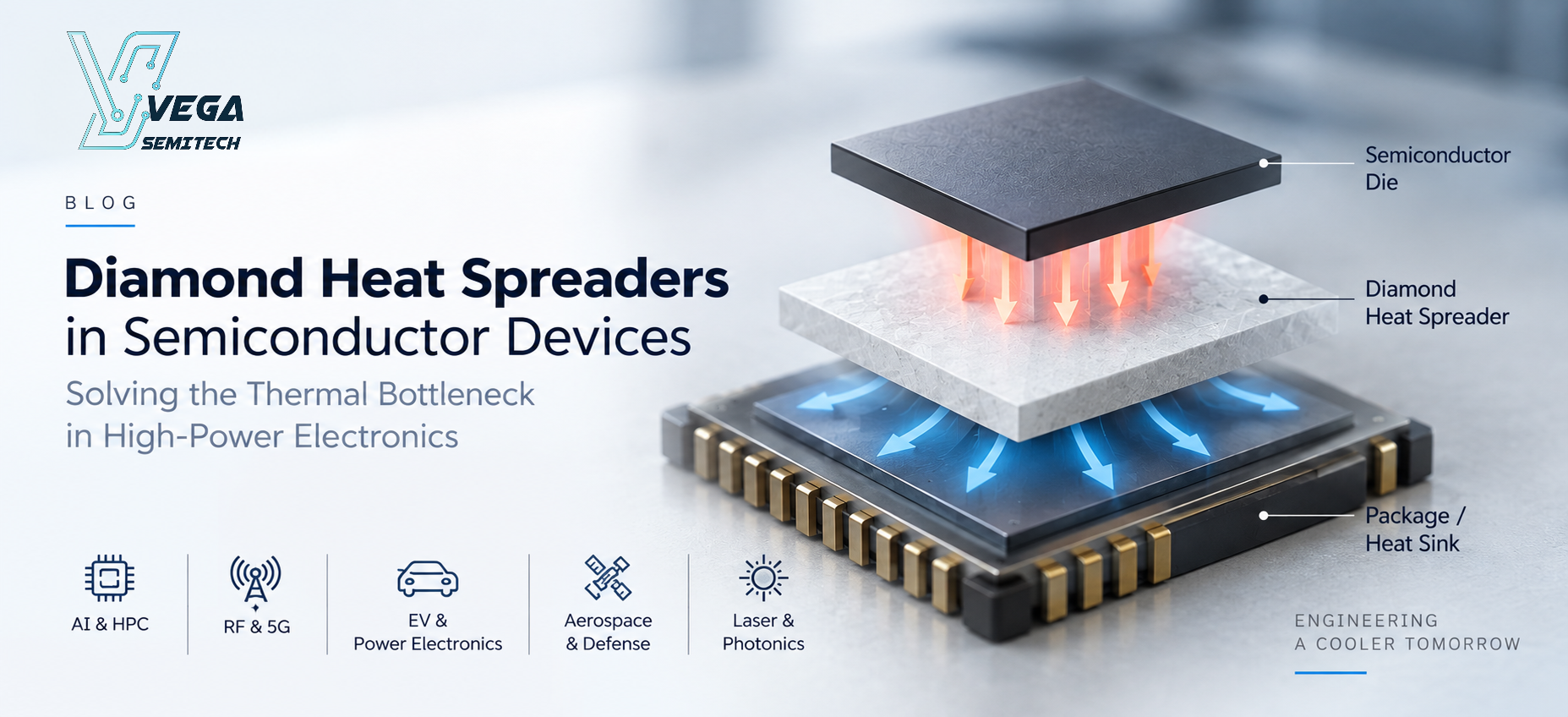
Instead of allowing heat to remain concentrated underneath the semiconductor die, the diamond distributes thermal energy laterally and vertically toward the package’s cooling structure.
A simplified thermal path can look like:
Semiconductor Die → Interface → Diamond Heat Spreader → Package / Heat Sink → Cooling System
By improving heat spreading close to the source, the entire cooling architecture can operate more effectively.
Why Diamond?
Diamond is much more than a gemstone. From an engineering perspective, it is an exceptional thermal material.
High-quality CVD diamond can provide extremely high thermal conductivity compared with many materials conventionally used in semiconductor devices and packaging.
This characteristic allows heat generated by a small, high-power semiconductor device to spread rapidly across the diamond layer.
The result can be:
- Reduced concentration of thermal hotspots
- Lower device junction temperature
- More uniform temperature distribution
- Improved device reliability
- Better performance under high-power operation
- Greater flexibility in high-density system design
For next-generation electronics, these advantages are becoming increasingly important.
Where Is the Diamond Heat Spreader Used?
A diamond heat spreader can be integrated into a semiconductor device or package in several configurations depending on the application.
Under the Semiconductor Die
One approach places the diamond heat spreader underneath the semiconductor die.
Device / Die
↓
Thermal Interface
↓
Diamond Heat Spreader
↓
Package / Cooling Plate
Heat generated by the active device passes into the diamond, which rapidly spreads it across a wider area before transferring it to the cooling structure.
This configuration can be particularly useful where a small semiconductor die generates a high heat flux.
Diamond Integrated Close to the Active Region
Advanced semiconductor architectures aim to position diamond even closer to the actual heat-generating region.
This is particularly relevant for GaN high-electron-mobility transistor (HEMT) technology, where extremely high power density can create localized hotspots near the transistor channel.
Reducing the thermal distance between the heat source and diamond can improve heat extraction, although interface engineering becomes critically important.
Diamond as a Substrate
Diamond can also function as a thermal substrate for semiconductor structures.
Architectures such as GaN-on-Diamond are being investigated and developed to combine the excellent electronic properties of GaN with the exceptional thermal properties of diamond.
Instead of managing heat only at the package level, this approach addresses thermal management much closer to the semiconductor itself.
Diamond Heat Spreaders for GaN Devices
GaN has become an important semiconductor material for high-frequency and high-power applications.
It is widely relevant to areas such as:
- 5G & 6G infrastructure
- RF power amplifiers
- Radar
- Satellite communication
- Aerospace
- Power electronics
One of the challenges with high-power GaN devices is self-heating.
As more power is generated within a smaller active area, localized device temperatures can rise rapidly. Diamond can provide a highly conductive thermal pathway for moving this heat away from the active region.
Research into GaN-on-diamond architectures has demonstrated the potential of diamond integration to significantly reduce device operating temperatures.
The opportunity is therefore not simply to create a better heat sink.
It is to bring an extremely high-performance thermal material closer to where the heat is actually generated.
Diamond Heat Spreaders for AI and High-Performance Computing
AI accelerators, GPUs and other high-performance processors are driving unprecedented levels of computing density.
More transistors and greater processing performance translate into increasingly challenging thermal loads.
Traditional cooling technologies—including advanced air cooling, liquid cooling and cold plates—remain important. But their effectiveness also depends on how efficiently heat can move from the chip into the cooling system.
Diamond heat spreaders can potentially improve this first stage of thermal transport.
A simplified architecture could be:
AI / HPC Chip
↓
Diamond Heat Spreader
↓
Package / Cold Plate
↓
Liquid Cooling System
Diamond does not necessarily replace the cooling system.
Instead, it can help the cooling system by spreading concentrated heat before it reaches the next thermal layer.
RF and Microwave Devices
High-power RF devices can generate intense localized heat while operating at high frequencies.
Temperature increases can negatively affect RF performance, efficiency and long-term reliability.
Diamond heat spreaders can therefore be particularly valuable for:
- RF Power Amplifiers
- GaN HEMTs
- Microwave Devices
- Radar Electronics
- Satellite Communication Systems
For these applications, thermal management can become an important factor in determining how much power can practically be extracted from the semiconductor device.
Laser and Optoelectronic Devices
High-power laser diodes and optoelectronic devices also require precise thermal management.
Localized temperature changes can influence optical performance, wavelength stability and component lifetime.
Diamond combines very high thermal conductivity with useful optical, electrical and mechanical properties, making engineered diamond materials attractive for demanding laser and photonics applications.
Power Electronics and EV Applications
Power semiconductor devices used in electric vehicles, charging infrastructure, industrial systems and renewable-energy equipment continuously handle large electrical loads.
GaN and SiC technologies are enabling smaller and more efficient power-conversion systems, but increasing power density also creates new thermal challenges.
Diamond-based heat spreaders and advanced diamond composites can provide another thermal-management option for future high-power modules where conventional materials begin approaching their practical limits.
The Interface Matters as Much as the Diamond
Simply adding diamond to a semiconductor package does not automatically guarantee maximum thermal performance.
The complete thermal pathway must be engineered carefully.
Important factors include:
- Diamond thermal conductivity — Material quality directly affects heat-transfer capability.
- Diamond thickness — The optimum thickness depends on device size, heat flux and package architecture.
- Surface quality — Flatness and surface finish influence bonding and thermal contact.
- Thermal interface resistance — Poor interfaces between the semiconductor, diamond and package can restrict heat flow.
- Coefficient of thermal expansion — Differences between materials must be considered to manage mechanical stress during temperature cycling.
- Bonding technology — The bonding layer should provide both mechanical reliability and efficient thermal transfer.
For this reason, semiconductor thermal management requires a system-level material and integration approach, rather than simply selecting the material with the highest thermal conductivity.
Diamond Is Moving Closer to the Chip
The semiconductor industry’s thermal-management strategy is evolving.
Traditionally, cooling focused primarily on moving heat from the package into a heat sink.
The next generation of thermal engineering is increasingly focused on addressing heat much closer to the semiconductor’s active region.
Diamond is uniquely positioned for this transition.
From CVD diamond heat spreaders and diamond substrates to GaN-on-Diamond and advanced metal-diamond composites, diamond-based materials can become an important part of next-generation semiconductor thermal architectures.
Vega Semitech: Engineering Diamond for Advanced Electronics
At Vega Semitech, we are developing semiconductor diamond materials and advanced thermal-management solutions for next-generation electronic applications.
Our focus includes engineered diamond materials for:
- Semiconductor thermal management
- High-power electronic devices
- AI and data-center hardware
- GaN and wide-bandgap semiconductor technologies
- RF and microwave electronics
- Advanced power electronics
- Next-generation semiconductor packaging
As semiconductor power density continues to increase, thermal performance will increasingly determine device performance.
Diamond provides a path to move heat faster, control hotspots and unlock higher-performance semiconductor architectures.
The future of high-power electronics may depend not only on how fast a device can compute or switch—but also on how efficiently it can move heat.