As power electronics move toward higher voltages, higher frequencies and greater power densities, semiconductor materials are being pushed beyond the limits of traditional silicon.
Gallium Nitride (GaN) has already emerged as an important wide-bandgap semiconductor for power electronics and RF applications. Diamond, meanwhile, is gaining attention as an ultra-wide-bandgap material with exceptional thermal properties and significant potential for future high-power devices.
But how do GaN and diamond actually compare?
Bandgap: Wide vs Ultra-Wide
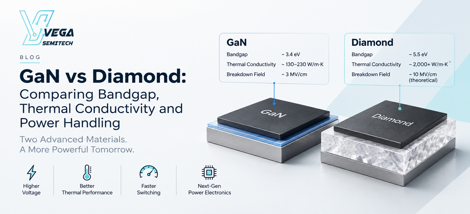
GaN has a bandgap of approximately 3.4 eV, significantly higher than silicon at around 1.1 eV. This wide bandgap contributes to GaN's ability to operate at higher electric fields, temperatures and switching frequencies than conventional silicon devices.
Diamond goes considerably further, with a bandgap of approximately 5.5 eV, placing it in the ultra-wide-bandgap semiconductor category.
A wider bandgap can enable devices designed for higher-voltage and high-temperature operation while helping reduce leakage under demanding conditions.
From a material-property perspective, diamond therefore offers considerable potential for extreme power electronics.
Thermal Conductivity: Where Diamond Stands Apart
Heat is one of the biggest challenges in modern semiconductor devices.
GaN has good thermal characteristics compared with many conventional semiconductor materials, but increasing power density can still create significant hotspots that limit device performance and reliability.
Diamond offers a major advantage here.
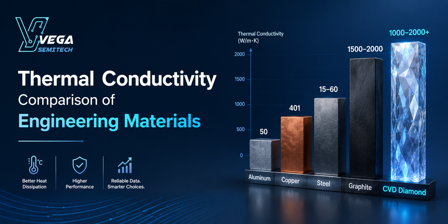
High-quality synthetic single-crystal diamond can exhibit thermal conductivity of roughly 2,000 W/m·K or higher, compared with approximately 130–230 W/m·K often cited for GaN depending on material quality and measurement conditions.
This exceptional ability to move heat is one reason diamond is being investigated not only as a semiconductor material itself, but also as a thermal-management material for GaN devices.
Power Handling
Another important material property is breakdown electric field.
GaN's high critical electric field has helped make it attractive for compact, high-voltage power devices. Diamond has an even higher theoretical critical electric field, giving it significant potential for future devices that need to withstand extreme electrical conditions.
This combination of:
- Ultra-wide bandgap + high breakdown field + exceptional thermal conductivity
makes diamond particularly interesting for next-generation high-power-density electronics.
However, excellent material properties alone do not determine commercial success.
If Diamond Is So Good, Why Are We Using GaN?
GaN technology has benefited from decades of semiconductor research, manufacturing development and commercialization.
Today, GaN devices are already being used in applications including power supplies, fast chargers, data centers, telecommunications, RF systems and automotive electronics.
Diamond semiconductor technology is much earlier in its commercialization journey.
Challenges remain around producing high-quality semiconductor-grade diamond wafers at scale, controlled doping, device fabrication, electrical contacts, integration, manufacturing yield and cost.
Therefore, diamond should not simply be viewed as an immediate replacement for GaN.
GaN + Diamond Could Be More Important Than GaN vs Diamond
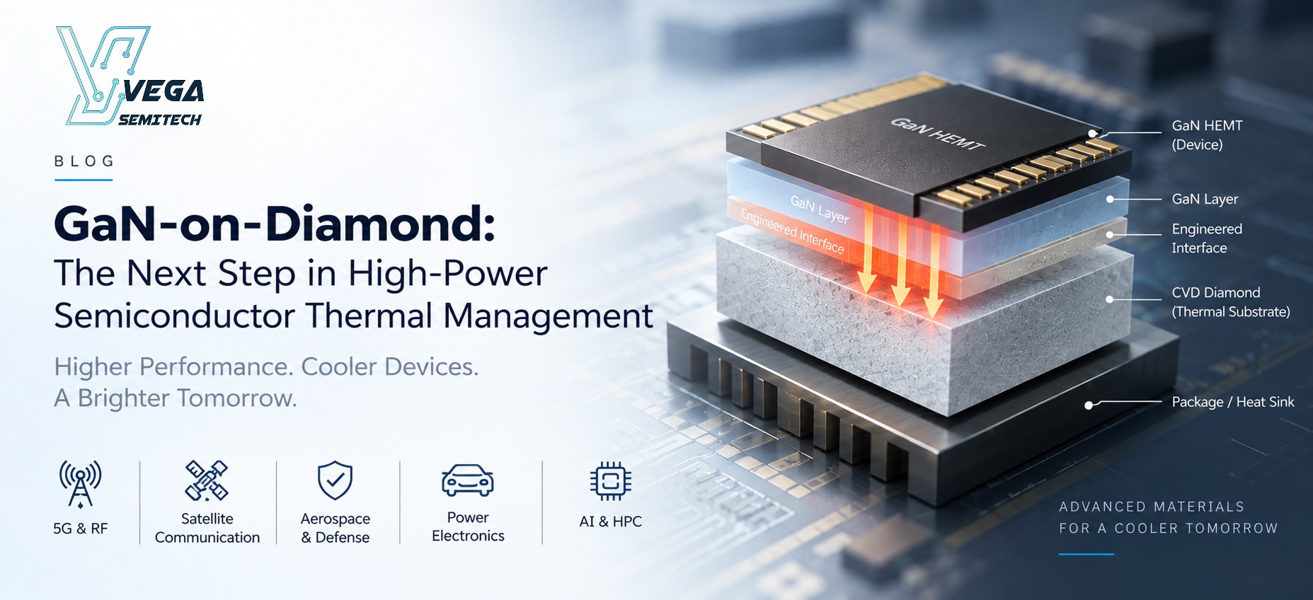
An especially interesting direction is GaN-on-Diamond.
Instead of choosing between the two materials, researchers and manufacturers can potentially combine their strengths.
GaN provides the active semiconductor layer with excellent high-frequency and high-power characteristics, while diamond can act as a highly effective thermal pathway beneath or near the active device.
The objective is straightforward:
Use GaN to handle the electronics and diamond to handle the heat.
Reducing the thermal resistance between GaN and diamond is therefore an important area of research. Better interfaces could allow heat generated within high-power GaN devices to move into the diamond layer more efficiently.
This could become increasingly important for RF power amplifiers, radar systems, satellite communications, data-center power infrastructure and other high-power-density applications.
GaN vs Diamond at a Glance
| Property | GaN | Diamond |
|---|---|---|
| Bandgap | ~3.4 eV | ~5.5 eV |
| Material Category | Wide Bandgap | Ultra-Wide Bandgap |
| Thermal Conductivity | ~130–230 W/m·K | ~2,000+ W/m·K |
| High-Frequency Capability | Excellent | Potentially Excellent |
| High-Power Potential | High | Extremely High Theoretical Potential |
| Commercial Maturity | Established and growing | Emerging |
| Manufacturing Ecosystem | Developing at commercial scale | Early-stage |
| Key Opportunity | Power & RF devices | Extreme power devices & thermal management |
Values are approximate and can vary substantially with crystal quality, structure, temperature and measurement method.
The Future May Be About Material Integration
The semiconductor industry's next major performance gains may not come from one material replacing another.
Instead, they may come from combining materials according to their strengths.
GaN already provides a strong platform for high-frequency and high-power electronics. Diamond brings exceptional thermal conductivity and promising ultra-wide-bandgap properties.
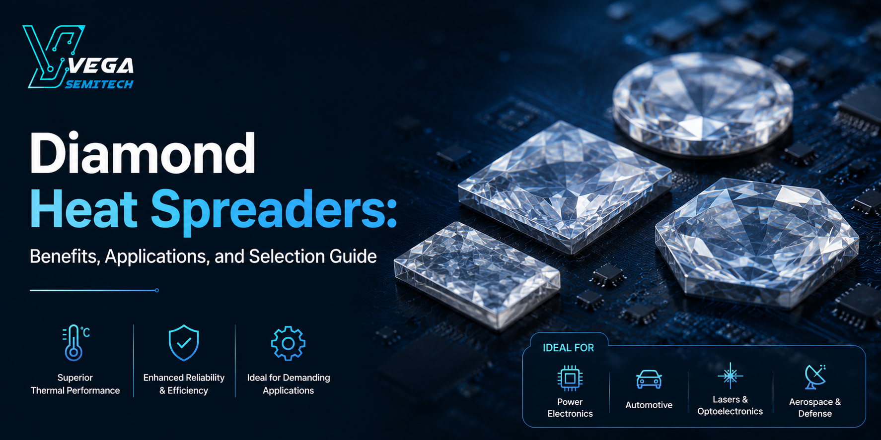
This makes technologies such as GaN-on-Diamond, diamond heat spreaders and eventually diamond-based semiconductor devices important areas to watch.
At Vega Semitech, we believe advanced semiconductor materials and thermal-management technologies will play an increasingly important role as electronics move toward higher power density, higher efficiency and more demanding operating environments.
The question may therefore be less about “GaN or Diamond?” and more about “How can GaN and Diamond work together?”